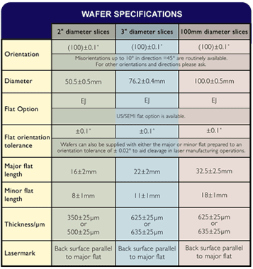
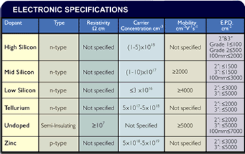
Mechanical
Specifications
Gallium arsenide can be supplied as ingots
or ingot sections or as-cut, etched or polished wafers. All
gallium arsenide wafers are individually laser scribed with
ingot and slice identity to ensure perfect tracability.
Packaging
Polished Wafers
Fluoroware type tray, individually sealed in two outer bags
in inert atmosphere. (Empak type boxes available on request)
As-cut Wafers
Empak type boxes (Glassine bag available on request)
‘Process Trial’ wafers
Fluoroware tray, individually sealed in one outer bag.
If you do not see
the specification you require,
please ask for details
|


Wafer Technology also offers GaAs wafers
produced by the High Pressure Liquid Encapsulated Czochralski
(LEC) method. Single crystal ingots are produced using high
purity gallium and arsenic as the starting material |