34 Maryland Road
Tongwell
Milton Keynes
Bucks
MK15 8HJ
United Kingdom
Telephone:
+44 (0)1908 210 444
Email: sales@wafertech.co.uk
![]() Wafer Technology Ltd.
Wafer Technology Ltd.
is a division of IQE plc www.iqep.com
© Wafer Technology Ltd. 2025
InP - Indium Phosphide
Wafer Technology offers single crystals that are grown in a pure fused silica system by the Czochralski method from multiple zone refined polycrystalline ingot.
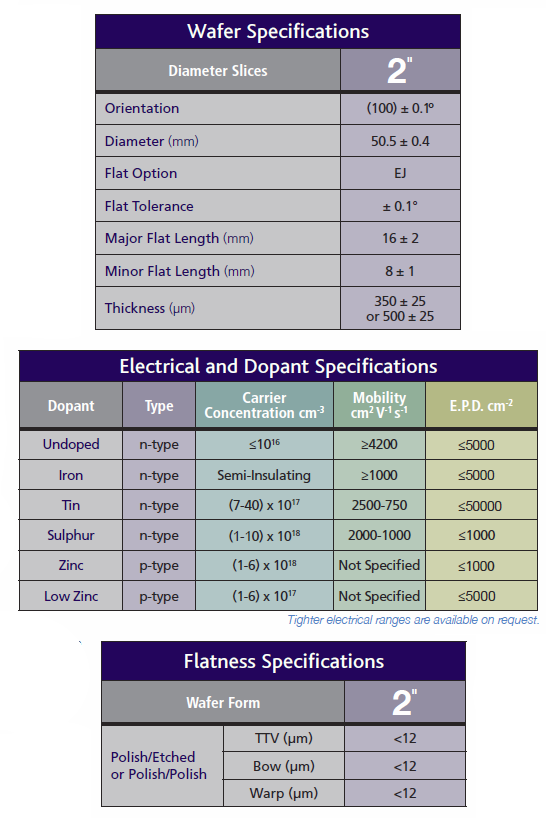
MECHANICAL SPECIFICATIONSIndium Phosphide can be supplied in as-cut, etched or polished wafer forms. All slices are individually laser scribed with ingot and slice identity to ensure perfect traceability. 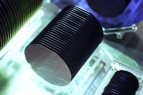 ORIENTATION SPECIFICATIONSSurface orientations are offered to an accuracy of +/- 0.05 degrees using a triple axis X-Ray diffractometer system. Substrates can also be supplied with very precise misorientations in any direction from the growth plane. Higher index substrates of the type (n,1,1) where n = 1,2,3,4,5,6 etc and orientations such as (110) are also available. We also offer wafers with cut and/or cleaved flats. SURFACE SPECIFICATIONSAll wafers are offered with high quality epitaxy ready finishing. Surfaces are characterised by in-house, advanced optical metrology techniques which include Surfscan haze and particle monitoring, spectroscopic ellipsometry and grazing incidence interferometry. PACKAGINGPolished Waferscoin-style tray, individually sealed in two outer bags in inert atmosphere. Cassette shipments are available on request). As-cut WafersCassette shipment. (Glassine bag available on request). 'Process Trial' wafersPackaged in coin-style wafer shipper, individually sealed in one outer bag. If you do not see the specification you require, please call for details on +44 (0)1908 210444 or email sales@wafertech.co.uk
|  | ||||

